Cadence unveils AI "Super Agent" for chip design, cuts verification to one day
Serge Bulaev
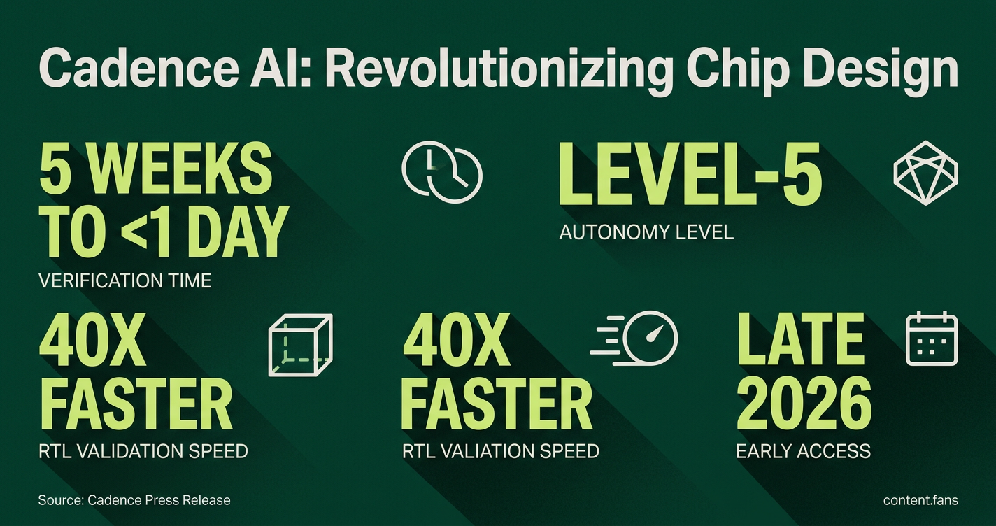
Cadence has announced an AI "Super Agent" for chip design, called ChipStack, which may reduce the time needed for chip verification from five weeks to less than a day. The new system is planned to be available for early customers in the second half of 2026 and combines Cadence's AI tools with NVIDIA models. Analysts suggest this could help chip projects test ideas more quickly, but real benefits might depend on how the system works in real production settings. Experts also note that the speed improvements could vary with different customers, and more information will come after actual case studies are released.

At Computex 2026, Cadence announced the industry's first fully autonomous virtual agentic AI design engineer, extending ChipStack AI Super Agent to Level-5 autonomy; Cadence says it reduces a typical five-week verification loop to less than a day. This new AI "Super Agent" aims to slash the standard five-week RTL verification cycle to under 24 hours. According to a Business Wire press release, early access is planned for the latter half of 2026.
Built upon Cadence's established AI-driven EDA portfolio, the new workflow integrates with NVIDIA Nemotron models within the secure OpenShell runtime. This collaboration points to an industry-wide shift toward governed, autonomous systems in semiconductor design.
Core Capabilities of the ChipStack AI Super Agent
The ChipStack AI Super Agent is a Level-5 autonomous system designed to handle complex chip verification tasks end-to-end. It collaborates with human engineers, allowing them to supervise and guide the process while the agent executes simulations, creates test benches, and manages coverage closure automatically.
Cadence's virtual engineer operates as an intelligent agent capable of planning, executing, and monitoring complex tasks across both simulation and formal verification. While it functions autonomously, it maintains a collaborative loop, allowing engineers to intervene and provide guidance. The system's architecture is based on three key pillars:
- Level-5 Autonomy: Manages key design tasks, including test-bench creation, simulation scheduling, and coverage closure, without direct human control.
- NVIDIA Foundation Models: Utilizes Nemotron models for advanced reasoning and code generation, operating within secure OpenShell sandboxes to protect intellectual property.
- Deep EDA Integration: Tightly integrated with Cadence's Xcelium logic simulation and Jasper formal engines, enabling what the company reports as "over 40x faster RTL validation cycles."
By targeting verification throughput, Cadence addresses a critical bottleneck in the chip design schedule. As noted by industry analysts in a Forbes report, this breakthrough could empower teams working on advanced SoCs to iterate more rapidly, although actual performance gains will hinge on specific production workloads.
Market Context and Competitive Landscape
According to industry reports, there is a clear trend in Electronic Design Automation (EDA) away from simple tool scripts and toward workflow-level autonomy, often involving multiple cooperating AI agents. Cadence's single-agent model aligns with this shift but stands out by claiming verified Level-5 autonomy, a move expected to pressure competitors to disclose their own progress in AI-driven design.
Industry observers suggest that a significant portion of enterprise applications may incorporate AI agents in the coming years. If this trend extends to the semiconductor sector, it will likely accelerate the adoption of secure, governed runtimes like OpenShell, which are essential for protecting sensitive design IP.
Key Adoption Factors to Monitor
Cadence says the Level-5 autonomous capabilities and AgentStack orchestration framework are expected to be available to early-access customers in the second half of 2026. Industry observers will be closely monitoring several key variables to gauge the system's real-world viability:
- The stability and reliability of code generated by Nemotron models when applied to large-scale, production-level designs.
- Seamless compatibility with existing regression suites and proprietary IP libraries crucial to customer workflows.
- The total cost of ownership (TCO) when compared to traditional, manual verification processes.
- The learning curve required for engineering teams to transition from direct task execution to a supervisory role overseeing the AI agent.
Experts advise that the dramatic speed improvements reported by Cadence may differ in practice due to customer-specific project constraints. Nonetheless, even partial success in accelerating verification could significantly reduce time-to-tapeout for complex designs like AI accelerators and automotive SoCs.
Broader Implications for the Semiconductor Industry
The collaboration between Cadence and NVIDIA aligns with broader agentic EDA trends, including the shift to cloud-native platforms and continuous feedback loops connecting design, manufacturing, and in-field performance data. By integrating large models with secure, accelerated computing, this partnership lays the groundwork for future AI agents to expand beyond verification into areas like physical design and yield optimization, assuming challenges in data governance and model accuracy can be overcome.
Currently, no customer case studies are available. Cadence is expected to release detailed performance metrics following the early-access program, which will provide a more transparent assessment of the AI agent's effectiveness across various production environments.